Samsung kickstarts LPDDR5 production using breakthrough process technology

Samsung has started mass production of LPDDR5 memory devices using its new process technology that uses extreme ultraviolet (EUV) lithography for some layers.
The South Korean giant is the first maker of dynamic random access memory (DRAM) to start applying EUV to production.
Samsung uses its 3rd generation 10nm-class process technology (also known as 1z) to make the industry’s first LPDDR5 memory chip featuring a 16Gb capacity. The chip supports a 6,400 MT/s data transfer rate, which is about 16% faster than that of Samsung’s 12Gb LPDDR5-5500 device.
Leading-edge memory
Samsung’s new DRAM allow the company to build 16GB memory modules for smartphones using only eight 16Gb devices. Today, a 16GB LPDDR5 stack uses 12 DRAM devices: eight 12Gb DRAMs and four 8Gb DRAMs.
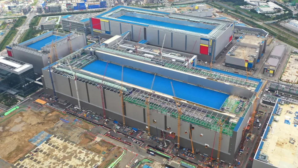
Samsung produces its 16Gb LPDDR5 memory devices at its second production line near Pyeongtaek, South Korea. The fab is used to make DRAM and will eventually be used to make V-NAND.

Right now, Samsung’s 3rd generation 10nm-class process technology is used to make only class-leading LPDDR5-6400 memory devices, but eventually the company will adopt the node to make other DRAMs, including DDR5 SDRAM.
Samsung said that it had already delivered the first 16GB LPDDR5 DRAM packages to ‘global smartphone makers’, so expect the first handsets that use the new memory devices shortly.
“The 1z-based 16Gb LPDDR5 elevates the industry to a new threshold, overcoming a major developmental hurdle in DRAM scaling at advanced nodes,” said Jung-bae Lee, executive vice president of DRAM Product & Technology at Samsung Electronics. “We will continue to expand our premium DRAM lineup and exceed customer demands, as we lead in growing the overall memory market.”